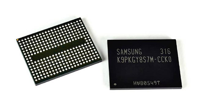
Samsung has started mass production of the industry’s first 3D Vertical NAND (V-NAND) flash memory, which can scale the limit of existing NAND flash technology and gain in performance and area ratio.
Today’s flash memory planar structure has a scaling limit due to cell-to-cell interference, while that shouldn’t be the problem with 3D V-NAND, plus the new structure also brings along performance enhancements.
The chip takes advantage of Samsung’s vertical cell structure based on 3D Charge Trap Flash (CTF) technology and vertical interconnect process technology to link the 3D cell array, which when combined offers twice the scaling of 20nm-class NAND flash available today.
Also, one of the most important technological achievements of the new Samsung V-NAND is that the company’s proprietary vertical interconnect process technology can stack as many as 24 cell layers vertically, using special etching technology that connects the layers electronically by punching holes from the highest layer to the bottom…
[Via: SammyHub]